Sign In
Upload
Manuals
Brands
NEC Manuals
Network Card
switch
NEC switch Ethernet Network Card Manuals
Manuals and User Guides for NEC switch Ethernet Network Card. We have
1
NEC switch Ethernet Network Card manual available for free PDF download: User Manual
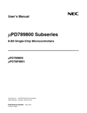
NEC switch User Manual (234 pages)
NEC User's Manua switch
Brand:
NEC
| Category:
Network Card
| Size: 2.01 MB
Table of Contents
Table of Contents
10
Chapter 1 General
21
Features
21
Applications
21
Ordering Information
21
Pin Configuration (Top View)
22
0S Series Lineup
23
Block Diagram
26
Functions
27
Chapter 2 Pin Functions
28
List of Pin Functions
28
Pin Functions
30
P00 to P07 (Port 0)
30
P10 to P17 (Port 1)
30
P20 to P26 (Port 2)
30
P40 to P47 (Port 4)
31
Reset
31
X1, X2
31
Regc
31
Usbdm
31
Usbdp
31
Vdd0 , Vdd1
31
Vss0 , Vss1
31
VPP ( Μ PD78F9801 Only)
32
IC (Mask ROM Version Only)
32
Pin I/O Circuits and Recommended Connection of Unused Pins
33
Pin I/O Circuits
34
Chapter 3 Cpu Architecture
35
Memory Space
35
Internal Program Memory Space
37
Internal Data Memory (Internal High-Speed RAM) Space
37
Special Function Register (SFR) Area
37
Vector Table
37
Data Memory Addressing
38
Processor Registers
40
Control Registers
40
Configuration of Program Counter
40
Configuration of Program Status Word
40
Configuration of Stack Pointer
42
Data to be Saved to Stack Memory
42
Data to be Restored from Stack Memory
42
General-Purpose Registers
43
Special Function Registers (Sfrs)
44
Special Function Register List
45
Instruction Address Addressing
48
Relative Addressing
48
Immediate Addressing
49
Register Addressing
50
Operand Address Addressing
51
Direct Addressing
51
Short Direct Addressing
52
Special Function Register (SFR) Addressing
53
Register Addressing
54
Register Indirect Addressing
55
Based Addressing
56
Stack Addressing
56
Chapter 4 Port Functions
57
Port Functions
57
Port Types
57
Functions of Ports
58
Port Configuration
59
Configuration of Port
59
Block Diagram of P00 to P07
60
Port 0
60
Block Diagram of P10 to P17
61
Port 1
61
Block Diagram of P20
62
Port 2
62
Block Diagram of P21
63
Block Diagram of P22
64
Block Diagram of P23 and P24
65
Block Diagram of P25
66
Block Diagram of P26
67
Block Diagram of P40 to P47
68
Port 4
68
Registers Controlling Port Function
69
Format of Port Mode Register
69
Format of Pull-Up Resistor Option Register 0
70
Port Mode Register and Output Latch Settings When Using Alternate Functions
70
Format of Port Output Mode Register 0
71
Format of Port Output Mode Register 1
71
Port Function Operation
72
Writing to I/O Port
72
Reading from I/O Port
72
Arithmetic Operation of I/O Port
72
Chapter 5 Clock Generator
73
Clock Generator Functions
73
Clock Generator Configuration
73
Block Diagram of Clock Generator
73
Configuration of Clock Generator
73
Register Controlling Clock Generator
74
Format of Processor Clock Control Register
74
System Clock Oscillators
75
System Clock Oscillator
75
External Circuit of System Clock Oscillator
75
Examples of Incorrect Resonator Connection
76
Frequency Divider
77
Clock Generator Operation
77
Changing Setting of CPU Clock
78
Time Required for Switching CPU Clock
78
Switching CPU Clock
78
Switching of CPU Clock
78
Maximum Time Required for Switching CPU Clock
78
Chapter 6 8-Bit Timer/Event Counters 00 and 01
79
Functions of 8-Bit Timer/Event Counters 00 and 01
79
Interval Time of 8-Bit Timer 00
79
Interval Time of 8-Bit Timer/Event Counter 01
79
Configuration of 8-Bit Timer/Event Counters 00 and 01
80
Block Diagram of 8-Bit Timer 00
80
Square Wave Output Range of 8-Bit Timer/Event Counter 01
80
Block Diagram of 8-Bit Timer/Event Counter 01
81
Registers Controlling 8-Bit Timer/Event Counters 00 and 01
82
Format of 8-Bit Timer Mode Control Register 00
82
Format of 8-Bit Timer Mode Control Register 01
83
Format of Port Mode Register 2
84
Operation of 8-Bit Timer/Event Counters 00 and 01
85
Operation as Interval Timer
85
Interval Time of 8-Bit Timer 00
85
Interval Time of 8-Bit Timer/Event Counter 01
85
Interval Timer Operation Timing of 8-Bit Timer 00
86
Interval Timer Operation Timing of 8-Bit Timer/Event Counter 01
86
Operation as External Event Counter (Timer 01 Only)
87
Timing of External Event Counter Operation (with Rising Edge Specified)
87
Operation as Square-Wave Output (Timer 01 Only)
88
Square-Wave Output Range of 8-Bit Timer/Event Counter 01
88
Timing of Square-Wave Output
89
Notes on Using 8-Bit Timer/Event Counters 00 and 01
90
Start Timing of 8-Bit Timer Counter
90
Timing of External Event Counter Operation
90
Chapter 7 Watchdog Timer
91
Watchdog Timer Functions
91
Inadvertent Loop Detection Time of Watchdog Timer
91
Interval Time
91
Watchdog Timer Configuration
92
Block Diagram of Watchdog Timer
92
Configuration of Watchdog Timer
92
Registers Controlling Watchdog Timer
93
Format of Timer Clock Select Register 2
93
Format of Watchdog Timer Mode Register
94
Watchdog Timer Operation
95
Operation as Watchdog Timer
95
Inadvertent Loop Detection Time of Watchdog Timer
95
Operation as Interval Timer
96
Interval Time of Interval Timer
96
Chapter 8 Usb Function
97
USB Overview
97
USB Bus Topology (Desktop Type PC)
97
USB Function Features
98
USB Function Configuration
98
Configuration of USB Function
98
Block Diagram of USB Function
99
Block Diagram of USB Timer
100
Configuration of Receive Token Bank
102
Configuration of Receive Data Bank
103
Configuration of Transmit Data Bank 0 (Buffer 0)
104
Configuration of Transmit Data Bank 1 (Buffer 1)
105
Configuration of TIDCMP and ADRCMP
107
Configuration of DIDCMP
108
Registers Controlling USB Function
109
Format of USB Receiver Enable Register
109
Format of Data/Handshake Packet Receive Mode Register
110
Format of Packet Receive Status Register
112
Format of Data/Handshake Packet Receive Result Store Register
113
Flag of RXSTAT after Reception of USB Reset Signal and Resume Signal
113
Format of Token Packet Receive Result Store Register
114
Format of Data Packet Transmit Reservation Register
115
Format of Handshake Packet Transmit Reservation Register
116
Conditions in Transmit Reservation
117
Configuration of Handshake Packet Transmit Reservation Register
119
Format of USB Timer Start Reservation Control Register
120
Format of Remote Wakeup Control Register
121
USB Function Operation
122
USB Timer Operation
122
Flowchart of USB Timer Operation
123
Remote Wakeup Control Operation
125
Flow Chart of Remote Wakeup Control Operation
125
Configuration of Remote Wakeup Control
126
Interrupt Request from USB Function
127
Interrupt Sources
127
Timing of Data/Handshake Packet Receive Interrupt Request Generation
127
List of Sources of Interrupts from USB Function
127
Timing of INTUSBRE Generation
128
Cautions When Using Interrupts
129
USB Function Control
130
Relationship between Packets and Operation Modes
130
Interrupt Servicing Flow
136
USB Function Internal Circuit Operations
140
Operation of Transmit/Receive Pointer
140
Flowchart of Transmit/Receive Pointer Operation
140
Receive Bank Switching ID Detection Buffer Operation
147
Flowchart of Receive Bank Switching ID Detection Buffer Operation
147
Sync Detection/Usbclk Detector Operation
148
Timing of Sync Detection/Usbclk Detector Operation
148
Timing of Sync Detection/Usbclk Generation Operation
148
Flowchart of Sync Detection/Usbclk Detector Operation
149
NRZI Encoder Operation
150
Timing of NRZI Encoder Operation
150
Flow Chart of NRZI Encoder Operation
150
Bit Stuffing/Strip Controller Operation
151
Timing of Bit Stuffing/Strip Controller Operation
151
Flow Chart of Bit Stuffing Control Operation
152
Flow Chart of Bit Strip Control Operation
153
Serial Interface 10
154
Chapter 9 Serial Interface 10
154
Functions of Serial Interface 10
154
Configuration of Serial Interface 10
155
Block Diagram of Serial Interface 10
156
Register Controlling Serial Interface 10
157
Format of Serial Operation Mode Register 10
157
Operating Mode Settings of Serial Interface 10
158
Operation of Serial Interface 10
159
Operation Stop Mode
159
3-Wire Serial I/O Mode
160
Wire Serial I/O Mode Timing
161
Chapter 10 Regulator
162
Block Diagram of Regulator and USB Driver/Receiver
162
Chapter 11 Interrupt Functions
163
Interrupt Function Types
163
Interrupt Sources and Configuration
163
Interrupt Source List
164
Basic Configuration of Interrupt Function
165
Registers Controlling Interrupt Function
166
Flags Corresponding to Interrupt Request Signals
166
Format of Interrupt Request Flag Register
167
Format of Interrupt Mask Flag Register
168
Format of External Interrupt Mode Register 0
168
Configuration of Program Status Word
169
Format of Key Return Mode Register 00
170
Block Diagram of Falling Edge Detector
170
Interrupt Servicing Operation
171
Non-Maskable Interrupt Acknowledgment Operation
171
Flowchart of Non-Maskable Interrupt Request Acknowledgment
172
Timing of Non-Maskable Interrupt Request Acknowledgment
172
Acknowledging Non-Maskable Interrupt Request
172
Maskable Interrupt Acknowledgment Operation
173
Interrupt Acknowledgment Program Algorithm
173
Time from Generation of Maskable Interrupt Request to Servicing
173
Timing of Interrupt Request Acknowledgment (Example of MOV A,R)
174
Multiplexed Interrupt Servicing
175
Example of Multiplexed Interrupt Servicing
176
Interrupt Request Hold
177
Chapter 12 Standby Function
178
Standby Function and Configuration
178
Standby Function
178
Register Controlling Standby Function
179
Format of Oscillation Stabilization Time Select Register
179
Standby Function Operation
180
HALT Mode
180
HALT Mode Operation Status
180
Releasing HALT Mode by Interrupt
181
Releasing HALT Mode by RESET Input
182
Operation after Release of HALT Mode
182
STOP Mode
183
STOP Mode Operation Status
183
Releasing STOP Mode by Interrupt
184
Releasing STOP Mode by RESET Input
185
Operation after Release of STOP Mode
185
Chapter 13 Reset Function
186
Block Diagram of Reset Function
186
Reset Timing by RESET Input
187
Reset Timing by Overflow in Watchdog Timer
187
Reset Timing by RESET Input in STOP Mode
187
Hardware Status after Reset
188
Μ Μ Μ Μ PD78F9801
190
CHAPTER 14 Μ Μ Μ Μ PD78F9801
190
Flash Memory Characteristics
191
Programming Environment
191
Environment for Writing Program to Flash Memory
191
Communication Mode
192
Communication Mode Selection Format
192
Communication Mode List
192
Example of Connection with Dedicated Flash Programmer
193
Pin Connection List
194
On-Board Pin Processing
195
Signal Conflict (Input Pin of Serial Interface)
196
Abnormal Operation of Other Device
196
Signal Conflict (RESET Pin)
197
Connection of Adapter for Flash Writing
198
Wiring Example for Flash Writing Adapter with 3-Wire Serial I/O
198
Wiring Example for Flash Writing Adapter with Pseudo-3-Wire Method
199
Chapter 15 Instruction Set
200
Operation
200
Operand Identifiers and Description Methods
200
Description of "Operation" Column
201
Description of "Flag Operation" Column
201
Operation List
202
Instructions Listed by Addressing Type
207
Chapter 16 Electrical Specifications
210
Chapter 17 Package Drawings
219
Chapter 18 Recommended Soldering Conditions
220
Surface Mounting Type Soldering Conditions
220
Appendix Adevelopment Tools
221
A-1 Development Tools
222
Software Package
223
A.1 Software Package
223
Language Processing Software
223
Control Software
224
A.3 Control Software
224
Flash Memory Writing Tools
224
Debugging Tools (Hardware)
225
Debugging Tools (Software)
226
Notes on Target System Design
227
A-2 Distance between In-Circuit Emulator and Conversion Adapter
227
A-3 Connection Condition of Target System (NP-H44GB-TQ)
228
Appendix Bregister Index
229
B.1 Register Index (Alphabetic Order of Register Name)
229
B.2 Register Index (Alphabetic Order of Register Symbol)
231
Appendix C Revision History
233
Advertisement
Advertisement
Related Products
NEC S401-AVT
NEC SVP SERVER -
NEC Nighthawk SX 4000D
NEC Univerge SV9100
NEC Storage Manager
NEC UNIVERGE SV9100 DT750
NEC SL-SYS-HOTEL LIC
NEC SpectraView II LCD1980FXi
NEC SpectraView II LCD2190UXi
NEC SpectraView II LCD2190UXp
NEC Categories
Monitor
Projector
Server
Telephone
Computer Hardware
More NEC Manuals
Login
Sign In
OR
Sign in with Facebook
Sign in with Google
Upload manual
Upload from disk
Upload from URL